





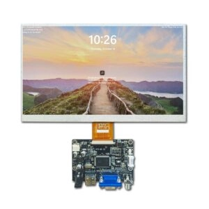
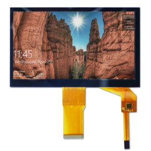


Electrostatic discharge (ESD) reliability should be addressed before an industrial TFT LCD module is frozen into the mechanical and electrical design. A module can perform correctly on a bench and still fail after installation because the final enclosure, touch layer, bezel, cable routing, and grounding arrangement create a new discharge path.
The most reliable approach is to treat the display as part of the complete product interface. Engineers should define the ESD environment, map possible discharge entry points, design a controlled return path, review protection at each interface, and validate the module in the final assembly. This checklist provides a practical design-in process for OEM engineering and procurement teams.

1. Define the ESD Design Scope
Start with the equipment environment rather than the display size or resolution. Before requesting samples, document how the operator interacts with the product and which parts of the display assembly are accessible.
Record:
- Equipment installation environment
- Indoor, outdoor, mobile, or fixed use
- Operator touch points
- Exposed glass, bezel, frame, and fasteners
- Touchscreen requirement
- Cable and connector locations
- Enclosure material and surface finish
- Expected temperature and humidity range
- Power architecture and display interface
- Planned assembly and service access
An industrial TFT LCD module installed behind an insulating cover does not have the same ESD exposure as a touch module mounted flush with a conductive front panel. The same display can therefore require different protection depending on the final product construction.
Create a short design brief that defines the expected failure modes. These may include temporary image disturbance, touch interruption, controller reset, communication loss, abnormal current, or permanent damage. Each failure mode should have a responsible engineer and a planned verification method.
For broader background on general display ESD risks, engineers can also consult Miqidisplay’s ESD protection guide for displays. The present checklist focuses specifically on design-in decisions and validation evidence.
2. Map Every Possible Discharge Entry Point
The display face is only one possible entry point. Build an ESD path map for the complete module and its surrounding assembly.
Inspect:
- Touch surface and cover lens
- Glass edges and corners
- Bezel openings
- FPC tails and exposed contacts
- Board-to-board and wire connectors
- Backlight wiring
- Display data cables
- Cable shields
- Mounting screws and brackets
- Ventilation openings near the module
- Gaps between the display and enclosure
The purpose of the map is to identify where a discharge can couple into sensitive conductors and where the current should flow instead. A protection feature is effective only when it provides a controlled, low-impedance path away from vulnerable circuits.
Flush-mounted displays deserve particular attention. A discharge applied near the frame may travel through a bezel, adhesive, conductive coating, or mounting hardware before reaching panel electronics. The edge construction, compression, gap, and grounding arrangement should therefore be reviewed as one mechanical and electrical system.
3. Establish a Controlled Grounding Architecture
“Grounded” is not a complete design description. The design record should show which conductive parts connect to chassis reference, which shields connect to circuit reference, and where high-frequency discharge current returns.
Review these questions:
- Is the metal bezel connected to a defined reference?
- Does the enclosure provide a short path to chassis or protective earth where applicable?
- Are display cable shields terminated consistently?
- Can discharge current pass through the display signal ground?
- Are mounting points intentionally conductive or only mechanical?
- Do the return paths contain long, narrow, or inductive sections?
- Are separate ground domains connected at a controlled location?
Avoid routing ESD current through sensitive display signals, touch-controller traces, reset lines, or low-voltage regulator nodes. The grounding strategy should be checked at schematic, PCB layout, cable drawing, and enclosure drawing level.
If the final equipment uses isolated or floating power, evaluate the ESD return path under the real installation condition. A laboratory bench connection may not represent the installed product.
4. Protect Interfaces at the Point of Entry
Protection components are generally most effective when placed close to the connector or other point where a discharge can enter. Long traces between the connector and protection device add inductance and can allow voltage to rise before clamping becomes effective.
For every interface, document:
- Signal type and operating voltage
- Normal data speed and edge rate
- Common-mode and differential-mode behavior
- Protection-device capacitance
- Leakage and clamping characteristics
- Placement relative to the connector
- Ground connection length and width
- Compatibility with the display controller and host electronics
Potentially exposed interfaces may include power, backlight control, display data, touch communication, reset, enable, and auxiliary control lines. The suitable protection approach depends on the electrical design and must be checked against the module and host specifications.
Do not assume that adding a transient suppressor automatically solves the problem. An unsuitable device can introduce signal distortion, leakage, startup problems, or an ineffective discharge path. Component selection, PCB layout, cable construction, and enclosure grounding must be validated together.
For example, an interface review for a 7-inch LVDS TFT LCD panel should include the FPC direction, connector location, cable length, shield arrangement, and clearance from conductive mechanical parts.
5. Review Touch and Cover-Glass Construction
A touch layer changes the ESD design because conductive sensing structures are located near the user-accessible surface. The cover lens, adhesive, sensor pattern, flex tail, controller, and surrounding frame should be reviewed as one assembly.
Confirm:
- Touch-sensor routing and shield strategy
- Sensor-tail location
- Controller placement
- Separation from display-interface lines
- Conductive coating or shielding, if used
- Mechanical clearance around the active area
- Adhesive coverage and edge conditions
- Contact between the cover structure and enclosure
The final ESD result depends on the complete equipment construction, including the customer’s enclosure and cable routing. A display supplier can provide module drawings and integration information, but the OEM remains responsible for validating the finished assembly.
For a custom project, request an outline drawing that shows active area, connector position, FPC direction, mounting features, and touch-related constraints. Miqidisplay’s custom TFT LCD display selection guide can help teams organize those requirements before sample selection.
6. Create a Revision-Controlled Design Record
Before approving a sample, create an ESD design record that connects each requirement to objective evidence.
Include:
- Product-level ESD requirement
- Intended test configuration
- Contact and air-discharge points
- Display module revision
- Touch and cover-glass revision
- Enclosure revision
- Cable and connector revision
- Grounding diagram
- Protection-device references
- PCB layout evidence
- Open risks and responsible owners
- Test equipment and calibration status
- Pass/fail criteria
- Deviation and corrective-action history
Revision control is essential. A panel substitution, revised FPC, altered cover glass, different adhesive, or modified bezel can change the discharge path even when the display size and resolution remain unchanged.
7. Validate at Module, Subassembly, and Product Level
Testing only the loose module may miss failures created by the final enclosure. Testing only the completed product can make it difficult to identify the source of a failure. Use three validation levels.
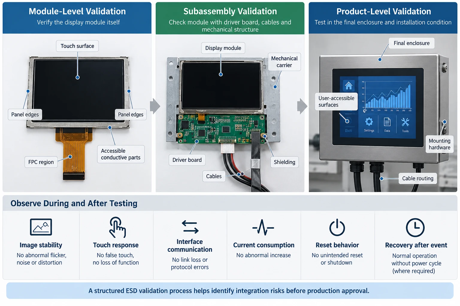
Module-level validation
Check exposed panel edges, touch surfaces, FPC regions, connectors, and accessible conductive features using a controlled fixture. Record the module revision and fixture geometry.
Subassembly validation
Test the display with its intended driver electronics, cables, shielding, and mechanical carrier. Observe image stability, touch response, interface communication, current consumption, and reset behavior.
Product-level validation
Test the final equipment in its intended enclosure and operating configuration. Include realistic mounting hardware, cable routing, power source, software state, and user-accessible surfaces.
The exact discharge levels, polarities, repetitions, test points, and acceptance criteria should be defined by the applicable product requirement and test method. A generic voltage value should not be presented as a universal pass condition.
8. Define Functional and Post-Test Acceptance Criteria
A pass/fail decision should cover temporary behavior as well as latent damage risk.
Record whether the unit experiences:
- Image flicker or corruption
- Touch-coordinate errors
- Display blanking
- Controller reset
- Host communication interruption
- Backlight shutdown
- Abnormal current
- Permanent pixel or line defects
- Loss of function after repeated events
- Recovery without operator intervention
Define the observation period after testing. Some failures are not visible during the discharge itself. A functional check, power-cycle check, interface check, and visual inspection may be required afterward.
For production approval, link the result to the exact display part number, firmware version, PCB revision, enclosure revision, and cable set. Otherwise, a later substitution may invalidate the evidence.
9. Include Handling and Packaging Controls
ESD control continues after laboratory validation. Modules can be damaged during receiving inspection, connector insertion, assembly, storage, and replacement.
Confirm:
- ESD-safe packaging and labeling
- Handling instructions for exposed FPCs
- Personnel grounding requirements
- Storage humidity and environmental limits
- Connector mating and unmating procedure
- Protective-film removal sequence
- Incoming inspection criteria
- Traceability by module revision and lot
These controls should be included in the supplier quality plan and assembly work instructions. They are especially important for modules with exposed contacts or touch-controller flex tails.
10. Prepare a Supplier Technical-Fit Review
A supplier can assess compatibility more effectively when the inquiry includes the complete integration context. Send:
- Display type and diagonal size
- Outline dimensions and active area
- Resolution and interface
- Touch requirement
- Brightness and viewing direction
- Operating temperature
- Mechanical constraints
- Connector and cable information
- Quantity and project stage
- Drawings or enclosure files
- Installation environment
- Known ESD test conditions
Miqidisplay’s verified product scope includes industrial TFT LCD panels and display modules in multiple sizes, interfaces, and configurations. For example, the 10.1-inch industrial TFT LCD panel provides a concrete reference for reviewing panel dimensions, interface placement, and integration constraints. The appropriate module, documentation package, sample plan, and customization scope must be confirmed for each project.
Conclusion
Industrial TFT LCD module ESD reliability is a system-design responsibility. The essential controls are clear entry-path mapping, intentional grounding, interface protection, touch and enclosure review, revision-controlled documentation, and staged validation.
Treat the display as an integrated component rather than an isolated panel. When ESD requirements are reviewed before the display, enclosure, cable routing, and PCB interfaces are frozen, engineering teams can identify vulnerable paths earlier, reduce sample rework, and create more defensible production-approval records.
FAQs
What is the first ESD design question for an industrial TFT LCD module?
Ask where a user can touch the equipment and where that discharge current is intended to flow. This reveals whether the display edge, bezel, touch layer, connector, or cable can become an unintended entry path.
Should ESD testing be performed on the loose display module?
Module-level testing is useful for identifying vulnerable regions, but it does not replace subassembly and product-level validation. The final enclosure and cable arrangement can materially change the discharge path.
Are protection components enough to prevent display ESD failures?
No. Protection devices must be matched to the signal, placed correctly, and connected to an effective return path. Mechanical construction, grounding, shielding, and layout are equally important.
What documentation should be requested before approving a display sample?
Request the interface drawing, connector and FPC details, mechanical outline, electrical specifications, handling guidance, and test-condition information relevant to the intended integration.
When should ESD requirements be reviewed with the display supplier?
Review them before the display, enclosure, cable routing, and PCB interfaces are frozen. Early review gives the supplier and system team time to address mechanical and electrical constraints together.
Request a Miqidisplay Technical-Fit Review
Send Miqidisplay your display type, diagonal size, outline dimensions, active area, resolution, interface, touch requirement, brightness, viewing direction, operating temperature, mechanical constraints, quantity, drawings, and integration environment. These inputs enable a component-compatibility review, identification of documentation and sample requirements, and assessment of possible customization needs for your industrial TFT LCD module project.
Email: mary@miqidisplay.com
WhatsApp: +86 189 6801 5464; +44 07892800850