









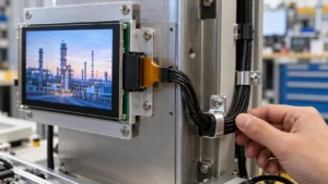

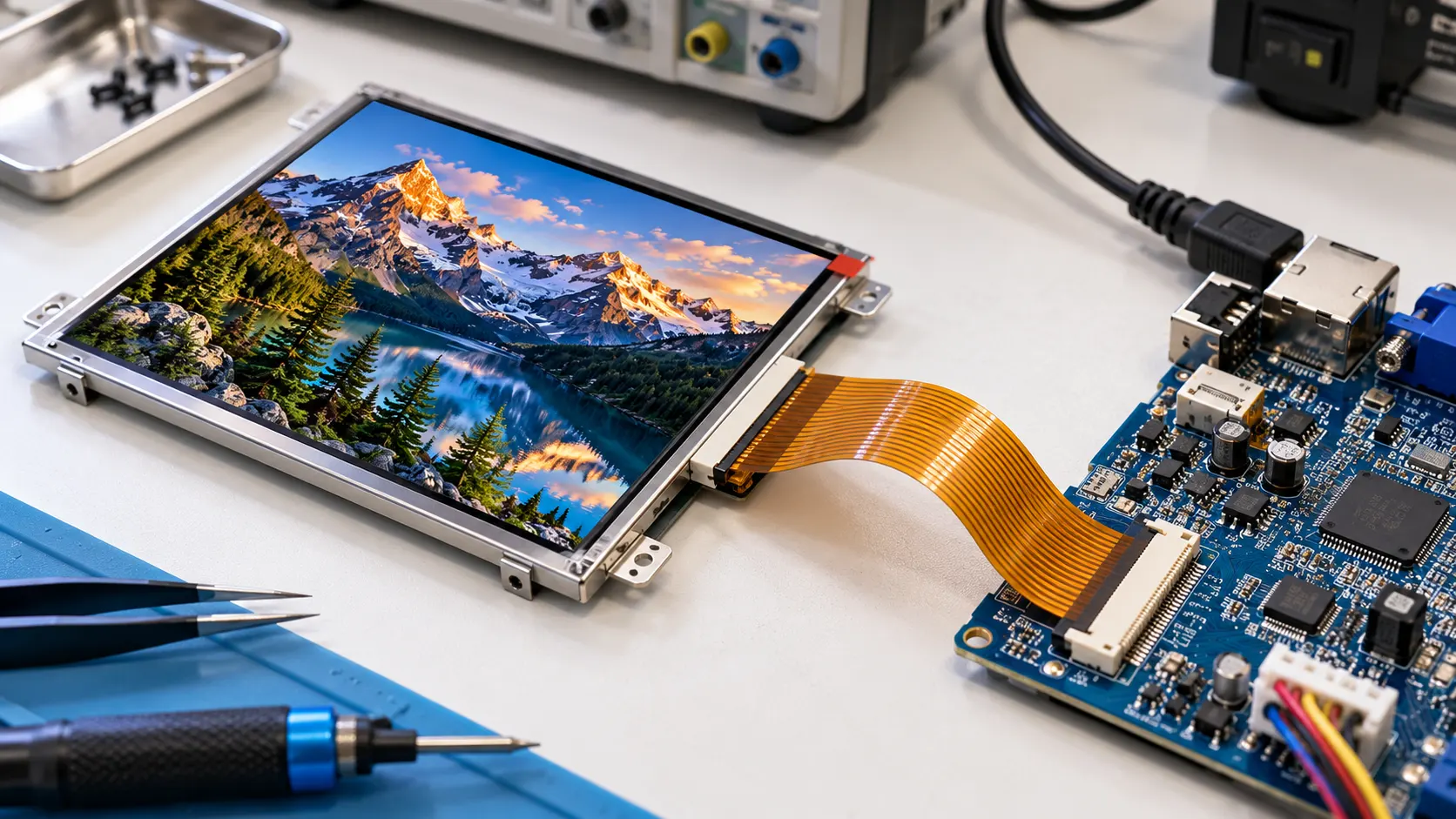
Electromagnetic interference (EMI) problems around a TFT LCD FPC and connector rarely come from one part alone. They appear when a fast display interface, flexible cable, connector transition, and host-board layout create an uncontrolled return-current path. The result may be artifacts, interference with nearby circuits, radiated-emissions failures, or a design that works on the bench but fails inside the final enclosure.
To reduce EMI risk around a TFT LCD FPC and connector, treat the cable and socket as part of the display interface—not as late-stage accessories.
For procurement and engineering teams, define the display interface, FPC construction, connector, grounding method, and verification conditions as one integration package.
1. Define the electrical architecture before requesting samples
Start with the interface, not the panel outline. MIPI, LVDS, RGB/TTL, SPI, and other interfaces have different edge rates, lane counts, pin assignments, and sensitivity to impedance discontinuities. A short, low-speed path may tolerate a simple FPC, while a longer multi-lane path needs tighter control of differential impedance, reference conductors, and connector geometry.
Put these items in the RFQ or design brief:
- interface type and lane or data configuration;
- expected cable length, bend direction, and connector orientation;
- host-board stackup and the available signal reference plane;
- display resolution, frame rate, and operating modes;
- touch, backlight, wireless, and switching-power circuits located nearby;
- enclosure materials and any intended chassis or frame ground.
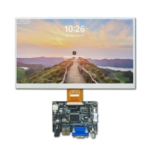
This information lets a supplier evaluate the display as an assembly rather than quote a panel with an unspecified cable. Miqidisplay’s TFT LCD display modules category shows that interface choices vary, so match the electrical interface to the host design before selecting size or brightness alone.
2. Control the signal path and its return path
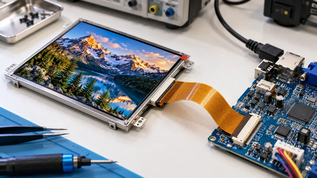
EMI risk rises when high-edge-rate signals leave a continuous reference plane, travel beside noisy power conductors, or pass through a poorly controlled connector transition. Keep the FPC short. Route it over a continuous ground reference on the host PCB, and avoid slots, cutouts, mounting holes, or plane splits under the connector and first cable section.
Avoid routing the display FPC in parallel with switching-node copper, inductors, motor wiring, radio traces, or high-current backlight paths. If it must cross a noisy region, cross quickly and at a controlled angle. Keep the bend away from connector contacts, and do not twist the FPC as it enters the socket.
Mechanical routing and EMI control are connected. Use the supplier’s cable strain-relief guidance to define support points, bend limits, and connector load path. A cable that moves or presses against the socket can change coupling and ground contact between builds.
3. Specify the FPC construction, not only the pin count
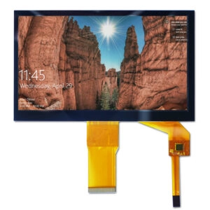
An FPC drawing should identify more than pitch and total pins. Ask for layer arrangement, signal-to-ground relationship, differential-pair geometry where applicable, contact finish, stiffener area, and shield or ground conductors. Place ground contacts beside or between high-speed signal groups where possible, and reserve a clear reference route through the connector.
The stackup must be compatible with the host-board transition. If an impedance-controlled pair widens, changes layers, or loses its reference at the breakout, the cable specification alone will not prevent EMI. Ask for the proposed pinout and mechanical drawing early enough for PCB review.
Shielding can help, but a floating foil or braid is not automatically an EMI solution. Define its termination and reference—chassis, digital ground, or a controlled connector shield. Avoid a long pigtail that adds inductance. If the product uses a metal frame or conductive gasket, document its electrical connection rather than assuming physical contact is a reliable RF reference.
4. Treat the connector as part of the RF path
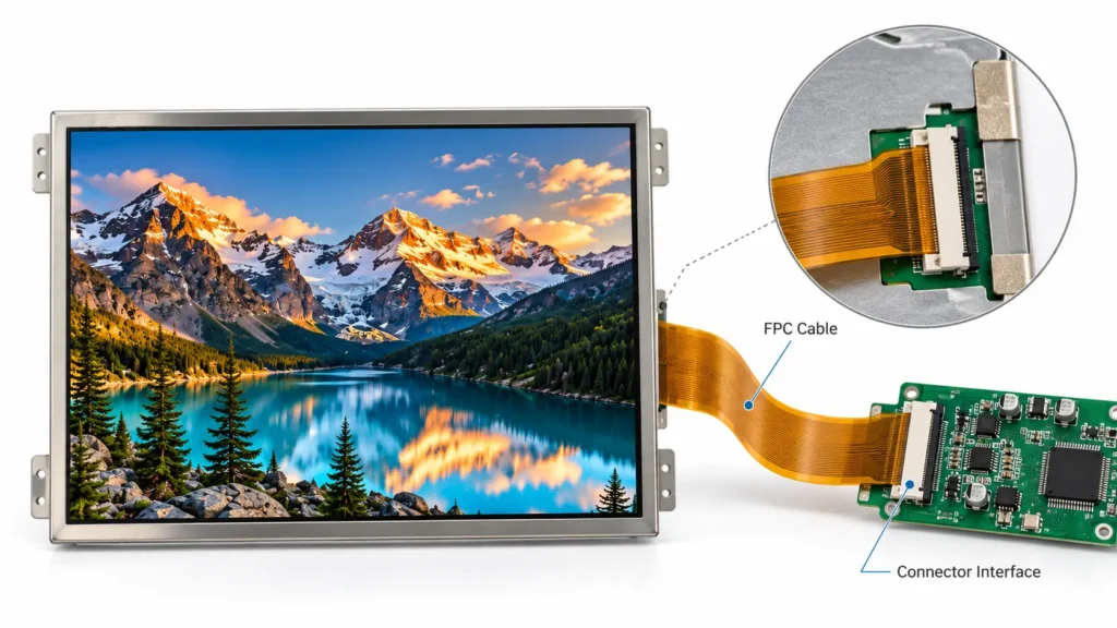
The connector is a discontinuity in both signal and return-current paths. Select a family that supports required pitch, mating cycles, insertion direction, FPC thickness, and contact arrangement. Review the assembled transition: host pads, contacts, ground pins, shell or shield, and nearby enclosure metal.
Keep high-speed contacts grouped with their references. Avoid placing a noisy power pin beside a sensitive differential pair when possible. If the connector is rotated or moved for packaging, re-check the pinout and return path.
Miqidisplay identifies cable, interface, connector, PCB, and mounting customization as custom-solution areas. Its custom cable and connector options are useful when a standard FPC orientation or pin arrangement creates avoidable EMI risk. Tie customization to a defined interface and enclosure requirement, not a vague “shielded cable.”
5. Separate display, touch, and power coupling
Many display assemblies include touch or backlight circuits near the image interface. Keep their routes and return currents organized so switching current does not share a narrow return path with high-speed image lanes. Where possible, separate display data, touch communication, and power entry along the cable and connector.
Do not add common-mode chokes, ferrite parts, or series resistors simply because EMI is suspected. They can reduce a specific noise mechanism but also reduce eye margin, change rise time, or disturb timing. First identify common-mode radiation, differential ringing, ground bounce, or adjacent-circuit coupling. Then evaluate filtering or damping with signal-integrity measurements at the actual interface speed.
6. Verify in the final mechanical configuration
A prototype that passes on an open bench is not enough. Test the selected TFT LCD module with the production-intent host PCB, FPC length, connector, mounting pressure, enclosure, display content, backlight level, touch activity, and nearby wireless or power circuits. Record cable route and chassis contact so the test is repeatable.
Use a staged review:
- Inspect the pinout, stackup, connector transition, and reference planes.
- Check signal quality at the receiver under the fastest intended mode.
- Compare radiated and conducted behavior with the enclosure open and closed.
- Move the cable within its permitted route to identify coupling sensitivity.
- Repeat across temperature and supply conditions that affect the interface or backlight.
If formal EMC testing is planned, agree in advance on the operating modes, cable position, grounding configuration, and pass criteria. The supplier should know which observations are required before the sample is approved, while the buyer should retain ownership of system-level compliance.
7. Put EMI requirements into the procurement package
An effective RFQ makes the risk visible. Include display size and active area, resolution, interface, touch requirement, brightness target, viewing direction, temperature range, outline, mounting constraints, FPC length, connector orientation, and quantity. Add pinout, lane assignment, expected data rate, reference-ground strategy, shield termination, and restricted routing zones.
Maintain a controlled record of assumptions and approvals. The LCD interface assumptions record can help align the host-board owner, supplier, mechanical designer, and compliance engineer before drawings are frozen. Require written notice of substitutions that change connector location, FPC layers, contact assignment, or shield construction.
Conclusion
Reducing EMI risk around a TFT LCD FPC and connector is an integration discipline. Define the interface early, preserve a continuous return path, control the FPC and connector transition, separate noisy power paths, and verify the complete assembly in its enclosure. Shielding and filtering support—not replace—a coherent layout and grounding strategy. RFQ-level requirements let buyers compare suppliers before tooling or compliance testing.
For a display choice that fits the electrical and mechanical constraints, request a Miqidisplay technical fit review with the interface, FPC route, connector orientation, enclosure, and verification conditions.
FAQs
Does a longer TFT LCD FPC always create EMI problems?
No. Length increases exposure to coupling and insertion loss, but outcome also depends on interface speed, stackup, reference continuity, connector transition, and nearby noise sources. A defined longer path can outperform a short path with poor return-current control.
Should the FPC shield connect to digital ground or chassis ground?
There is no universal answer. Termination depends on enclosure, host grounding, safety requirements, and frequency range. Define the reference and test it in the assembled product; do not leave the shield floating by default.
Can a supplier change the connector orientation after the RFQ?
Only with documented approval. Orientation changes can alter the bend, pinout, return path, and proximity to noise. Re-review the PCB footprint, cable route, and enclosure clearance before accepting the change.
What should be included with a first display sample?
Request the actual FPC, connector, pinout, mechanical drawing, available stackup information, and shield or grounding notes. Test it with the intended host board and enclosure, not a substitute cable.