OLED (Organic Light Emitting Diodes) screens shine by passing electric current through RGB organic materials placed between electrodes. Since these displays glow on their own, they don’t need backlights like LCD screens do. This makes them much thinner, bendable, and better at saving power. OLEDs stand out with their slim, adaptable shape, light build, and sharp, clear pictures.
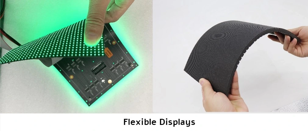
Especially, flexible OLED displays use bendable materials like polyimide instead of rigid glass. They can fold or roll, which is why more people want them for mobile gadgets. This amazing tech is now common in smartphones, wearables, and foldable screens.

Flexible Substrate Formation
A special liquid called Varnish is spread on carrier glass and heated to create a bendable base (PI). Varnish: Polyamic acid solution (a starter for PI). This polyimide layer acts as the main support for the whole display setup. The method often uses precise tools like the Coater Line (SK-P Series) to make sure the surface is even and free of flaws.
Backplane Formation
A backplane, made of TFTs (thin film transistor circuits) and banks (small walls for organic glowing layers), is built on the bendable base. This backplane works as the control system for each tiny dot on the OLED screen. It makes sure the light comes out just right.
TFT Formation Process
Cleaning
The base is carefully washed to get rid of tiny dust bits and leftover grime. First, it’s cleaned with pure water and sound waves. Then, a dry plasma method finishes the job for a spotless surface. Tools like the Cleaning Processor (TS Series) use automatic brushes and strong water jets to make the base perfect. This step is super important for making good screens without errors.
Deposition
Thin layers, often made of soft silicon or metal stuff like IGZO, are added using a spraying method for wires or a gas-based process (PECVD) for insulators. Things like gas flow (e.g., SiH4 for PECVD) and heat (200–300°C) are watched closely. This helps keep the layer thickness steady (10–100 nm) and avoids any mistakes.
Resist Coating
A light-sensitive layer is put on with a slit-nozzle tool (SK-E Series). This layer, about 1–2 µm thick, is spun at 1000–1500 rpm to spread evenly. Careful control of its stickiness and removing extra bits at the edges help make the coating perfect. This is key for tiny, accurate patterns.
Exposure
A sharp, high-quality tool shines UV light (365 nm) through a pattern mask to mark out circuits. The light amount (50–100 mJ/cm²) is set just right to change the layer only where needed. This allows for super small details, as tiny as 2 µm.
Development
The marked areas of the layer are washed away with a basic liquid (e.g., TMAH-based solutions) using a Coater Developer system. The time (30–60 seconds) and heat (23–25°C) are adjusted to avoid errors. This keeps the pattern edges nice and sharp.
Etching
Parts of the thin layer not covered are removed with wet solutions (e.g., HF-based for oxides) or dry methods (reactive ion etching with CF4/O2 plasma). The speed of removal (10–50 nm/min) is controlled to protect the layers below and shape the transistors just right.
Resist Stripping
Any leftover layer is taken off with special liquids or oxygen plasma. Doing this at 80–100°C makes sure everything comes off without harming the TFT setup underneath. This gets the base ready for the next steps.
Bank Formation Process
Resist Coating
A light-sensitive polyimide mix is spread to make small walls. The slit-nozzle coater keeps the thickness even (1–3 µm). This is really important for setting the borders of each dot during RGB placement.
Exposure
UV light hits the layer through a super accurate mask to shape the walls with tiny precision. The light strength is tweaked based on the layer’s thickness and how sensitive the material is.
Development
The marked spots are washed away to build walls, usually 1–2 µm tall. Several rounds of light and removal steps smooth out the wall shapes. This ensures straight sides and neat spaces for adding organic stuff accurately.
Organic Light Emitting Layer Formation
RGB organic stuff is turned into vapor in a super empty space (10⁻⁶ Torr) and placed through a thin metal mask (FMM) with holes as small as 20 µm. Heat-based methods keep the layer thickness steady (10–50 nm). This is key for even color and brightness. New ideas, like inkjet printing, are being tested for bigger production. But they need exact control of drops to stop colors from mixing.
Thin Film Encapsulation (TFE)
TFE uses layers of organic material (printed polymers, 5–10 µm thick) and hard stuff (Al2O3 or SiNx via PECVD, 50–100 nm). This mix of layers keeps water vapor out (WVTR below 10⁻⁶ g/m²/day). It protects the OLED from breaking down while staying bendable.
Touch Sensor Panel Formation
Cleaning
The base is washed with water and plasma to clear away tiny bits. This makes sure the touch layers are free of flaws.
Deposition
Clear conductive materials (e.g., ITO) are sprayed to form touch sensor points. The layer thickness (20–50 nm) and resistance (10–50 Ω/sq) are set for good touch response and clear view.
Resist Coating
A light-sensitive layer is added with a slit-nozzle coater. It spreads evenly for sharp touch patterns.
Exposure
UV light through a mask shapes the touch sensor layout. Tiny details down to 5 µm help with multi-touch features.
Development
The marked layer is washed off, showing the conductive part for the next step.
Etching
Wet or dry methods remove extra ITO, creating an exact sensor grid.
Resist Stripping
Leftovers of the layer are cleaned off, leaving a neat touch sensor tied to the display.
Formation of Color Filter Film with Anti-Reflection Function
Color filter films are added using a Coater Developer (SK-F Series) with RGB colors and anti-glare coatings (refractive index ~1.5). The exact thickness (1–2 µm) cuts down on shine while making colors and contrast better.
Flexible Substrate Delamination
A pre-step with laser lift-off (e.g., 308 nm excimer laser) loosens the base from the carrier. The glass is pulled off by hand, leaving a bendable OLED panel that can curve as tight as 3 mm. It’s now ready to be put into devices.
FAQ
Q: Why do flexible OLED displays not need backlights?
A: OLEDs glow by themselves, so they don’t need extra lights like LCDs. This leads to slimmer designs and stronger contrast.
Q: What makes polyimide suitable for flexible substrates?
A: Polyimide is great because it handles heat well, bends easily, and stays strong. These traits are perfect for the hot steps in making OLEDs.
Q: How do manufacturers protect OLED layers from environmental damage?
A: A protective film is made with vapor and inkjet methods. It blocks out water and air, which can harm the screen over time.
Custom Best Flexible OLED Displays from Miqidisplay: Popular Display Factory from China
Miqidisplay has become a trusted name in China for custom flexible OLED displays. They provide special solutions for medical, industrial systems, car dashboards, and security tools. Based in Shenzhen, Miqidisplay has over 20 years of solid experience in this field.
Miqidisplay is a trusted provider of advanced display technologies and solutions, offering a comprehensive portfolio including LCD, TFT, IPS, OLED displays, and specialized accessories.
Miqidisplay Flexible screens have good flexibility, light volume, low power consumption, and are resistant to rubbing. The sizes currently available are 1.03″, 2.07″,6.67″, 7.91″,12.6″. Contact us to send your inquiry today.